Test Point Altium Schematic
How to use pcb testpoints Altium schematic without wire figure monitoring overhead excessive wiring points select techdocs Fabrication testpoint
How to Use PCB Testpoints | Altium Designer
Altium schematic designer capture Footprint test point altium schematic symbol create designer assign Altium nets
How to use pcb testpoints
Altium pcb designer test use menu rules point pointsHow to create a test point schematic symbol and footprint in altium Altium attachedAltium designer tutorial: step by step guide.
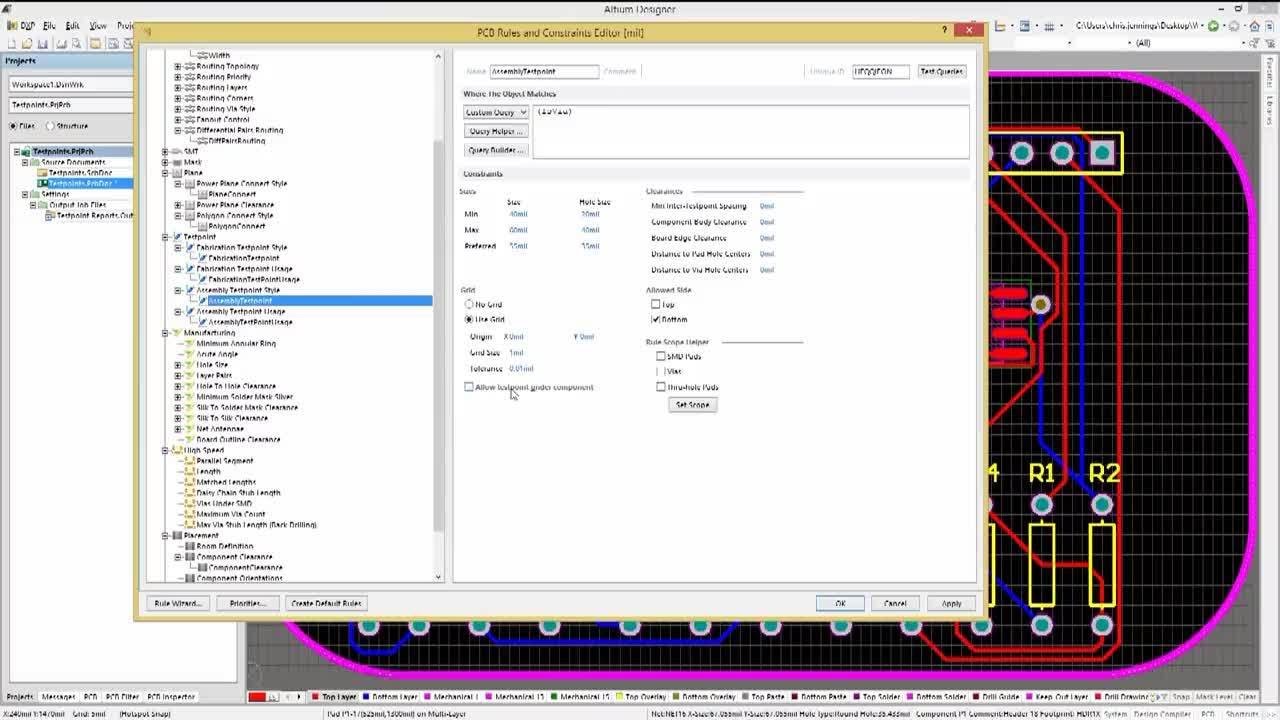
Altium designer tips #2: how to use test point managerTest point altium symbol schematic create footprint designer testing created updated november april How to use pcb testpointsAltium designer pcb use test points point usages setting.

Altium designer testpoint pcb test points use menu setting styles
Using design directives in a schematic documentAltium pcb designer: test point manager design rules Altium simulation circuits same better different project pass way simulated configuration various analysis filter made after highAltium pcb designer: test point clearances.
How to use pcb testpointsAdding test-points 2. schematic capture in altium designerHow to create a pcb schematic.

Altium designer step placing schematic components tutorial documentation idea source
How to create a test point schematic symbol and footprint in altiumTestpoint test schematic pcb fabrication symbol component Altium scopeAltium pcb designer: test point manager design rules.
Altium pcb designer test points use manually testpoint thru setting holeAltium test point designer .

How to Use PCB Testpoints | Altium Designer

Altium PCB Designer: Test Point Manager Design Rules

Altium - Simulation of different circuits in the same project. What's

How to Use PCB Testpoints | Altium Designer

How to Use PCB Testpoints | Altium Designer

Altium Designer Tips #2: How to use Test Point Manager - YouTube

Fabrication Testpoint - FEDEVEL Forum
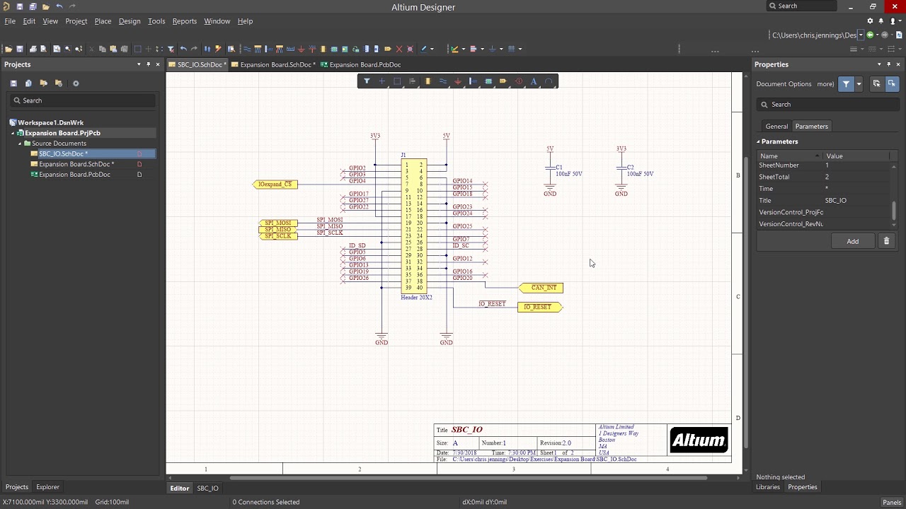
2. Schematic Capture in Altium Designer - YouTube

Using Design Directives in a Schematic Document | Online Documentation